
I. New course of perspective R&D Heterostructures, LED chips and white LEDs on their base
The developed technology allows to organize mass production of high-performance LED chips on the base of blue light emitting In-Ga-N heterostructures. Process has been developed in collaboration with "IF Tethys" (St. Petersburg) and Ioffe Institute of Russian Academy of Science. Mass production of chips is being developed at the center of LED technology in Tomsk.
The main structural feature of presented heterostructure is the application of the principle of short-period superlattice for design of epitaxial layers of heterostructure. It has been extensively tested in practice in previous generations of LED chips produced by JSC "IF Tethys" and successfully working in the white LEDs on dozens of facilities and objects of Russian Railways and of Housing and Public Utilities (St. Petersburg).
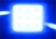
The most promising today topology of flip-chip ensures its stable operation in a range of high power consumption - from 1 to 5 watts. The introduction of original "know-how" allows to achieve values of the external quantum efficiency comparable with world-famous analogues - 35 to 45%.
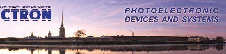
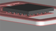
The development of the modern mass production of white LEDs based on the proposed blue light emitting chips is planned. The LED is developed in full compliance with the concepts of consumer demand in present and in the near future. This is a white LED on a flat two-sided square ceramic SMD package with a lens and a phosphor layer formed on the basis of highly stable silicone compounds. Luminous efficacy of LED in comfortable warm (2700-3500 K) and neutral (3500-5000 K) white colors will be, respectively, 100-120 and 110-130 lm / W at standard 350 mA.
Also there will be launched the production of LED modules and fixtures to address the implementation of projects of internal and external lighting for industrial and office buildings and street lighting.
II. Large format CCD resistant to space ionizing radiation
At the moment the development of array CCD with 1024×1024 is carrying out and based on it photodetector for high-precision electro-optics systems of spacecrafts (SC) astro-orientation, goniometers, operating in high radiation conditions (up to 5•105 rad by γ -radiation) for visible and near IR ranges.
During the work must be accomplished the following tasks:
• development of the design and circuitry of photodetector, providing the fulfillment of requirements in survivability and resistance to external influences (GOST RV 20.39.414.1 with additions);
• development of product reliability testing methods and conduction of accelerated testing for reliability (150.000 hours) and persistence (25 years);
• development of modern technological processes allowing to implement technical requirements to the photodetectors;
• development of metrological and testing base for the photodetectors.
An important feature of this CCD is “KNOW-HOW” in the development of special radiation-resistant technology of CCDs manufacture and also the construction of the photodetector with the system of CCD crystal cooling, and its electronic control and output signal processing in digital form.
The deadline for completion of the development scheduled for late 2015 with the release of technical specifications and development of the device in production.
JSC "NRI "ELECTRON" invites your company to mutually beneficial cooperation.
JSC "National Research Institute "ELECTRON"
194223 RF, Saint-Petersburg, Toreza pr., 68, Tel/Fax: +7(812) 552-61-54, +7(812) 552-36-00; E-mail:info@electron.spb.ru